PASCAL Scoping of Nets
I must first apologize for the technical sounding name here, but I struggle to explain this feature to my colleagues and the best buzzword I came up with was “Pascal Scoping”.
What problem does this feature solve?
When designing op-amps and what we may call “conventional” analog chips it is likely that the design engineer never comes across the issue of isolated digital supplies. But when a large SOC (System on a Chip) is designed there is a need to provide separate power to various blocks. For example, imagine an Audio IO chip that has a Stereo ADC, a Stereo DAC and a PLL. This chip will typically have hundreds of thousands of gates to support the sigma delta modulators, digital filtering and clock generation. We find that the performance of the ADC and DAC is limited because it shares the same power supply as the digital filter and so we ask the layout team to please keep separate power supplies for the large logic block from the ADC or DAC.
However, this causes a problem in the methodology (in the “flow”) used to make the chip. It is common to use a standard library cell (a D Flip-flop for example) in the ADC or DAC [why? Because we don’t want to slow down the design process and unnecessarily design a new cell when a verified one is available] and this standard library cell has global names “VDD” and “VSS” attached to it just like the cells used in the digital filter. These globals having the same name are connected – the netlist simply cannot separate these nodes because they are the same name and they are declared global. The usual fix is to simply rename the cell and the global ports on the cell where they are used in the analog designs. This is what designers do, and it works and the chip gets to FAB and all is well. So for example, the VSS and VDD in the DAC DType cell become VSSDAC and VDDDAC and the cell becomes DTypeDAC.
However, that new cell with new named globals needs to be re-used – we want to make many chips with the same component parts for rapid turn time and risk reduction. Maybe the next chip has six Audio DACs not two and so the same problem occurs again – the stereo DAC is placed on the chip three times and again has its power connected because they are the same named globals again. Pragmatically to get the job done the designer again creates four more different global names and all is well. So now we have DAC1 with globals VSSDAC1, VDDDAC1, VSSDAC2 etc. You can see the problem I am sure. If that DAC fails or needs upgrade there are now three designs to edit.
How to solve this problem of needing to isolate global names?
One solution is dramatic: don’t use globals at all. Frankly this is impractical for two reasons: firstly, you cannot do everything yourself – the company will want to purchase IP (a digital cell library) and that will have globals. But secondly and to me more importantly, schematics are used to communicate design ideas and methods between analog engineers – a schematic is a like a chess game in progress: as an analog design engineer you will have evolved a ‘pattern recognition” process like the chess master and you can as easily see a “random” schematic as a chess player can see a random placement of the pieces on the board. So a schematic is not just a description to drive the layout tool to do the right thing, it is a work of art encapsulating intriguing and occasionally profound insights to share with our colleagues and the analog design community at large. It simply will not do to “clutter” it up with all those global wires that communicate little.
The ideal solution then would preserve the benefit of global wires (that they simplify a drawing) and at the same time do not force all similarly named global wires to be connected. This sounds paradoxical, but the same issue comes up in programming languages and one such language is PASCAL and PASCAL has a solution to this issue. Programmers use the word “scope” to refer to sections where a variable name is used and I implemented a concept similar to PASCAL’s notion of “global scoping” in the Schemata tool. In words it works like this: as you draw a schematic you may declare any wire to be a global and within that drawing all sub blocks if they also mention that global will be connected. However, when you drop that drawing with its global into a higher level drawing you may use the same global name but this time do not declare it as a global – declare it as a port or even as a local wire. At this point the global “stops propagating upward” and is “collected” at this level. It may then emerge as a port of any name and be connected in any way you wish. An example is needed: here is such an example, here I am demonstrating Schemata’s global scoping by using Schemata’s transparent icons – I think this makes it clear.
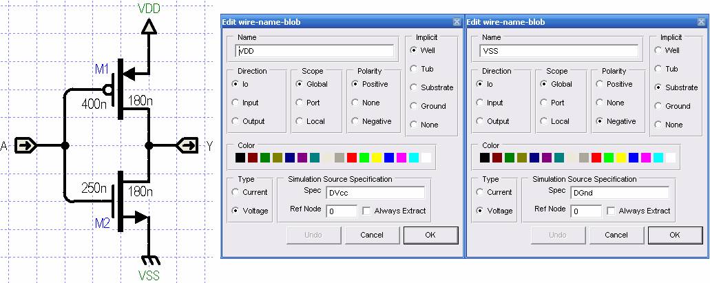
1) This is the inverter – note that VDD and VSS are globals. VDD is also declared to be of positive polarity and implicitly is the well connection. VSS is declared to be of negative polarity and implicitly the Substrate connection.

At this point the complete SPICE netlist is:
*Spice extract of Inv
*Note: Globals are Extracted as Ports in this Netlist
*From file Primitives:Logic;Inv.sch
.options accurate parhier=calibre nowarn
.lib mm018-dv.l RES
.lib mm018-dv.l BIP3
.lib mm018-dv.l TT_3V
.lib mm018-dv.l TT
.TEMP = 35.0
.param AVcc = 3.3
.param AGnd = 0.0
.param Dvcc = 1.8
.param Dgnd = 0.0
.param Gnds = 0.0
** Global VSS is ignored (because Globals are in port lists)
** Global VDD is ignored (because Globals are in port lists)
VVSS VSS 0 DGnd
VVDD VDD 0 DVcc
M1 Y A VDD VDD pch L=180.0n W=400.0n
M2 Y A VSS VSS nch L=180.0n W=250.0n
.end
There is no hierarchy here and globals are irrelevant at this level. Note however that the back-gate of the M1 is connected to VDD and the back-gate of M2 to VSS as expected because we indicate the well and the substrate in the net label properties.
2) Next we will use these inverters in a simple delay line

The netlist is now:
XZ1 A Z1_Y VSS VDD INV
XZ2 Z1_Y Y VSS VDD INV
.subckt INV A Y VSS VDD
M1 Y A VDD VDD pch L=180.0n W=400.0n
M2 Y A VSS VSS nch L=180.0n W=250.0n
.ends INV
.end
(I have deleted the irrelevant parts of the netlist)
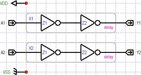
3) Now I am going to place two of these delay lines in a higher level design using transparent icons so that we can still see the inverters. Note that I have added two wires as globals VDD and VSS – these are our top level connections to the power.

The netlist is now
*Spice extract of delay2
*Note: Globals are Extracted as Ports in this Netlist
*From file Schematics:drawings;delay2.sch
.. ..
** Global VSS is ignored (because Globals are in port lists)
** Global VDD is ignored (because Globals are in port lists)
VVSS VSS 0 DGnd
VVDD VDD 0 DVcc
X1 A1 Y1 VDD VSS DELAY
X2 A2 Y2 VDD VSS DELAY
.subckt DELAY A Y VDD VSS
XZ1 A Z1_Y VSS VDD INV
XZ2 Z1_Y Y VSS VDD INV
.ends DELAY
.subckt INV A Y VSS VDD
M1 Y A VDD VDD pch L=180.0n W=400.0n
M2 Y A VSS VSS nch L=180.0n W=250.0n
.ends INV
.end
Note that VSS and VDD are connected, but the essential point is that they are connected as ports, not as globals – you don’t need to worry about it the connection is just as would have been if they were global, but in fact they are being passed as ports.
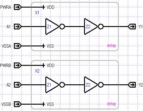
4) Now the interesting bit – suppose I want to use those inverters in the delay line but I want to separate the power supplies – how do I do it? Like this – add a wire named as the global but declared to be a port. I am going to show you two ways you can do this – the first on VSS I am going to just use the same name, on VDD I am going to use a different name – just to show the two possibilities:

The VDD wire is local and named VDD – it will collect all the global wires in the inverters named VDD. It then connects to a port called PWR – therefore a port named PWR will emerge from this design and is actually the connection to all the global VDD’s below. The VSS wire is a port and a local (the one on the right is a local) – there is nothing else on the wire – it will collect all the VSS globals below and emerge as a port named VSS
5) Here are our two delay lines – again using transparent icons to try to be clear.

(Perhaps you can see now why I added that local “VSS” on the right of the port wire – it just helps clarify the transparent icon)
Now the netlist is:
X1 A1 PWRA VSSA Y1 DELAY
X2 A2 PWRB VSSB Y2 DELAY
.subckt DELAY A PWR VSS Y
XZ1 A Z1_Y VSS PWR INV
XZ2 Z1_Y Y VSS PWR INV
.ends DELAY
.subckt INV A Y VSS VDD
M1 Y A VDD VDD pch L=180.0n W=400.0n
M2 Y A VSS VSS nch L=180.0n W=250.0n
.ends INV
.end
You can see the power is connected differently, (to PWRA, PWRB, VSSA, VSSB) as we want, and yet the schematic (named “delay”) is making use of globals to avoid having to draw power to the inverters.
Summary:
You have the option to use PASCAL scoping of globals – when you choose to do so you can use globals in your design and so make “nice looking” schematics. Those globals do not need to be all connected together – you can “collect” lower level globals into a port or local wire. The netlister (if PASCAL scoping is enabled) does not make use of globals – all your globals are passed as ports with the appropriate connections.